Band Switch for SSB 6.1 transceiver
I have an idea about building band commutator for SSB 6.1 transceiver. The board supposed to be connected by 14 pin ribbon cable between main transceiver board and DDS board.
I added some blocking capacitors because I discovered some RF noise induced by ribbon cable. I assume it was coming from PICs conntrollers installed on DDS board.
The very cool feature of that board in ability to chain with another such board. Imagine, if you need to commutate +5V, +12V and +27V. You can stack 3 such boards and here you go. The current PCB desing is not for high-voltage commutation but relays can commutate about 1 kW of power up to 240V which is nice for their price. I don't recommend to use current PCB design in high-voltage (please, don't do that, it could be fatal) design.
Schematic
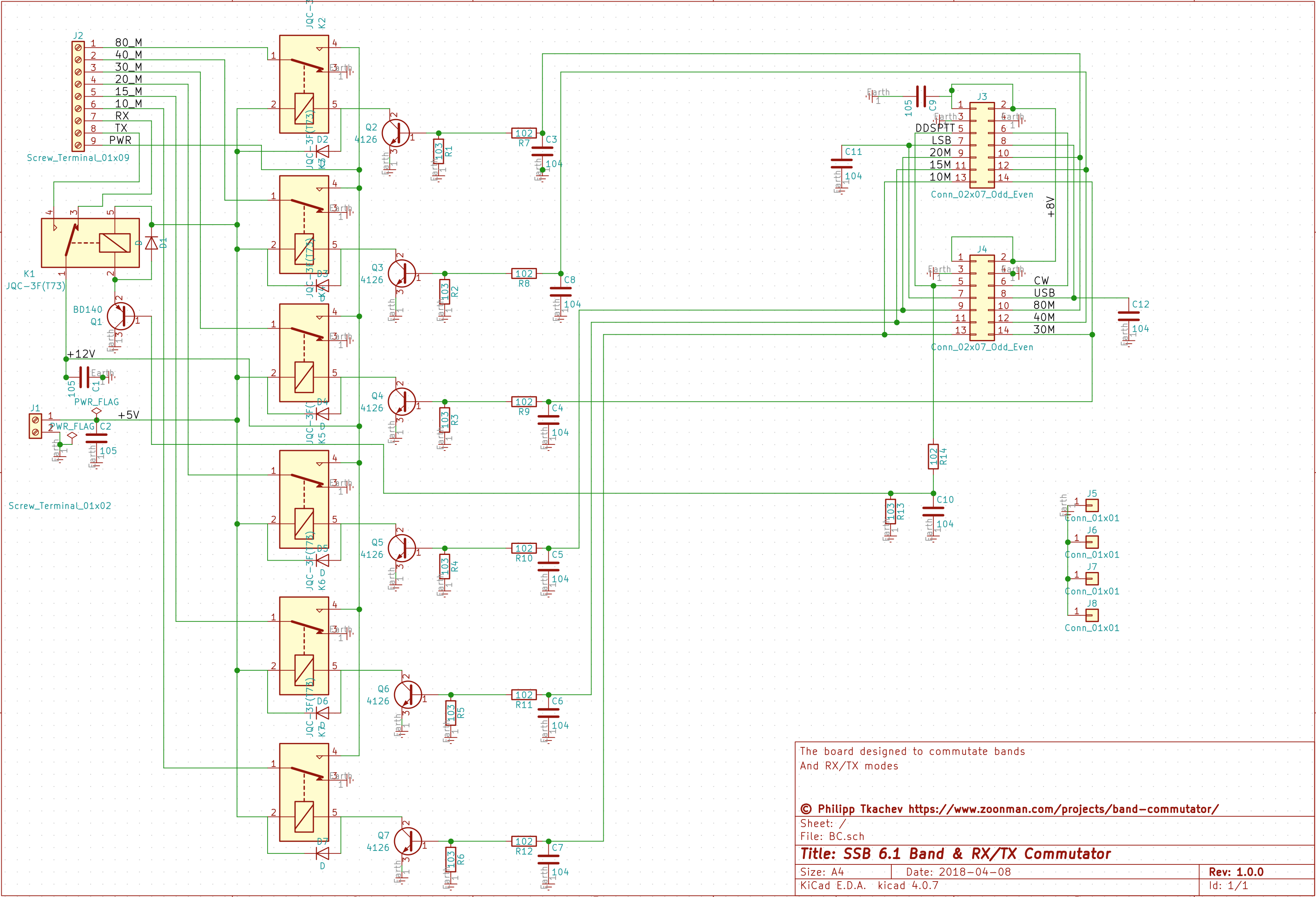
It has been drawn in KiCad v4.0.7.
There is nothing new from schematic design standpoint just a trivial switch.
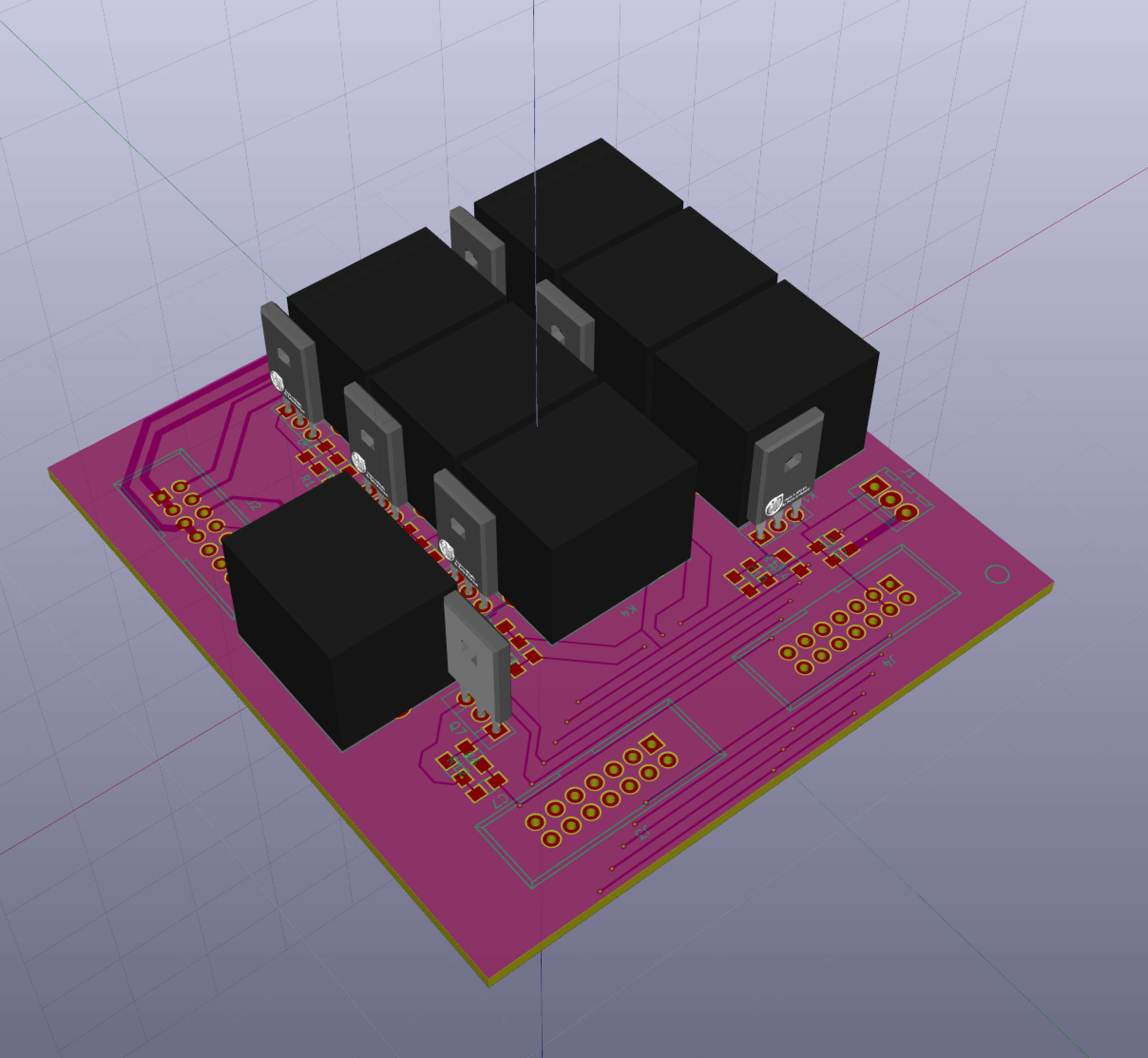
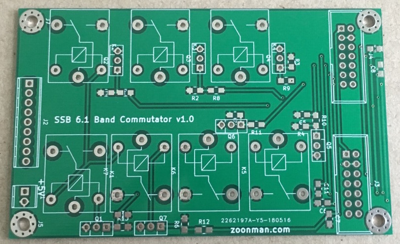
Board
 |
 |
 |
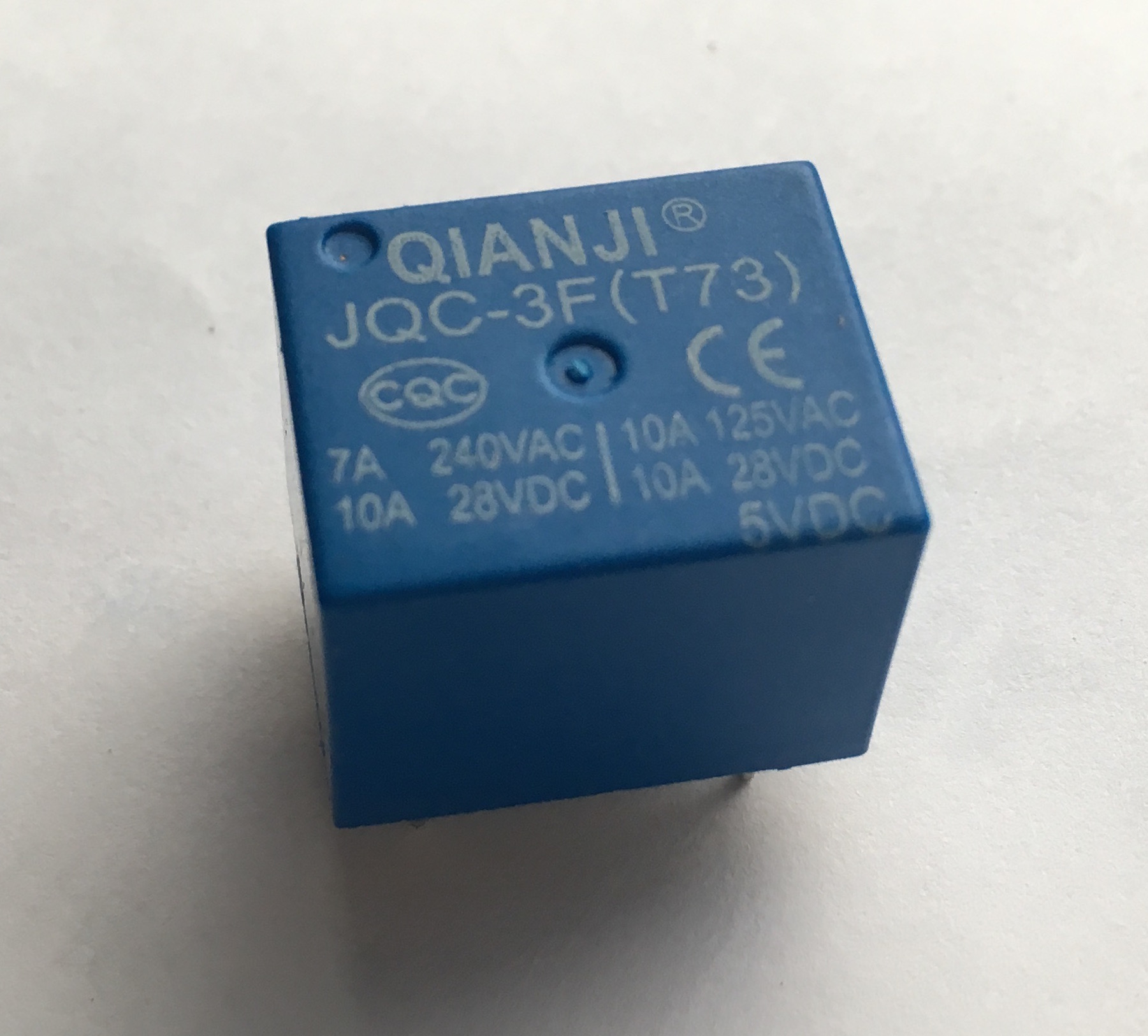
This board uses cheap JQC-3F relays from China and scavenged 4126PL transistors from CFL lamp ballasts. Fairly speaking all NPN transistors wich could operate the relay current (Icollector≥100mA) will work fine here. It is simple commutator. You can even substitute those with N-channel mosfets, those will work fine too.
|
|
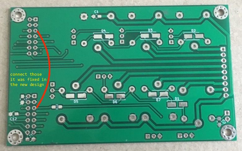
ERRATA
Use BD140 for Q1 because TX signal is coming inverted.
Install relays upsidedown. I recently found that they connect all lines to +12V by default. Looks like pin numbers on schematic didn't match actual connections in footprint.
Download band switch project ~170kB, zip.
Bill of materials
| Ref | Qnty | Value | Part | Datasheet | Description |
|---|---|---|---|---|---|
| C1, C2, C9 | 3 | 1 uF | C | Unpolarized capacitor | |
| C3, C4, C5, C6, C7, C8, C10, C11, C12 | 9 | 100 nF | C | Unpolarized capacitor | |
| D1, D2, D3, D4, D5, D6, D7 | 7 | D | D | Protection Diode | |
| J1 | 1 | Screw Terminal 01x02 | Screw Terminal 01x02 | Generic screw terminal, single row, 01x02 | |
| J2 | 1 | Screw Terminal 01x09 | Screw Terminal 01x09 | Generic screw terminal, single row, 01x09 | |
| J3, J4 | 2 | Conn 02x07 Odd Even | conn: Conn 02x07 Odd Even | Generic connector, double row, 02x07, odd/even pin numbering scheme (row 1 odd numbers, row 2 even numbers) | |
| J5, J6, J7, J8 | 4 | Conn 01x01 | conn: Conn 01x01 | Generic connector, single row, 01x01 | |
| K1, K2, K3, K4, K5, K6, K7 | 7 | JQC-3F(T73) | relays: JQC-3F(T73) | PCB Relay, +5V | |
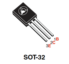
| Q1 | 1 | BD140 | Q PNP BEC | Transistor PNP (general) | |
| Q2, Q3, Q4, Q5, Q6, Q7 | 6 | 4126PL | Q NPN BCE | Transistor NPN (general) | |
| R1, R2, R3, R4, R5, R6, R13 | 7 | 10 k | R | Resistor | |
| R7, R8, R9, R10, R11, R12, R14 | 7 | 1 k | R | Resistor |
Checkout my design of SWR meter.
You can left first comment.